


Prepare the request around the board outline, circuit or attachment pattern, mating stack and validation method. The product name does not establish thickness, flatness, electrical behavior, thermal capability, metallization or certification, so those requirements must be specified separately.
Key Inquiry Requirements
Define the substrate architecture
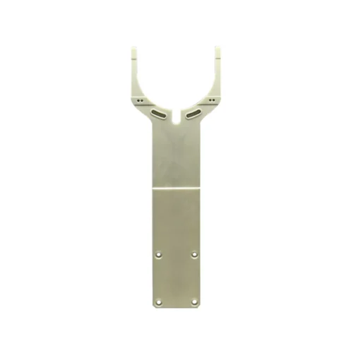
Start with the substrate’s role in the assembly and identify every functional face. Provide the outline, thickness intent, corner treatment, holes, slots, keep-outs and datum structure. Show whether the substrate is a single ceramic plate, a patterned circuit carrier or one element in a layered construction. The assembly drawing is often as important as the substrate drawing.
Include the mating parts, clamping or bonding method and the location of any heat source, sensor, connector or fastener. Indicate which surfaces require contact, clearance, insulation or attachment. A clear stack-up lets the supplier review fit and stress risks without inferring the design from a product title or a generic substrate category.
Specify material and surface requirements
AlN is a material family, but a substrate specification also depends on surface finish, flatness, edge condition and compatibility with the selected attachment process. State the approved material designation if one exists, or describe the required assembly environment and invite clearly identified options. Do not assume that all AlN substrates share the same processing or joining behavior.
Describe cleanliness, contamination limits, color or visual requirements, surface roughness and any restrictions on lapping, polishing or handling. If the substrate will be metallized or bonded, define the required surface zones and adhesion evaluation method. Keep material properties and compliance claims as explicit requirements that must be documented and verified.
Detail layout and metallization
For a patterned substrate, provide the conductor layout, pad dimensions, isolation gaps, registration marks, polarity indicators and edge clearances. Identify whether the layout is preliminary or controlled, and show critical dimensions in enlarged views. If metallization or another surface treatment is required, describe the layer locations, intended attachment process and inspection points without presuming a standard stack.
Coordinate the ceramic drawing with the circuit or module drawing so registration, warpage, pad location and component clearance are evaluated together. State how alignment will be measured and whether the buyer needs a coupon, sample panel or first-article review. The more precise the interface definition, the easier it is to distinguish ceramic geometry from downstream assembly variation.
Plan mechanical and electrical inspection
Define the dimensional checks that protect assembly fit: outline, thickness, flatness, hole location, edge profile, pad registration and surface condition. Add visual criteria for chips, cracks, contamination and unwanted marks. Identify the datum scheme and measurement method, because a tolerance without a reference frame may not control the installed relationship.
Electrical or functional checks should be written for the actual substrate design and attachment method. Depending on the assembly, the buyer may need continuity, isolation, adhesion, visual registration or thermal cycling evaluation. Treat each as a stated inspection or test requirement, and do not infer conductivity, dielectric performance or reliability from the AlN name alone.
Prepare a substrate RFQ
Send the controlled substrate drawing, circuit layout, stack-up, revision history and intended assembly process. Include expected project quantity, sample requirements, packaging needs and any restrictions on marking or surface contact. If the design is replacing an existing substrate, provide failure images, dimensional comparisons and the reason for the redesign or replacement.
Request a technical review that lists assumptions, proposed material definition, manufacturing route, metallization scope and inspection evidence. Compare quotations by interface completeness and validation plan, not only by ceramic shape. Before release, confirm the final layout, acceptance criteria and application test method so the substrate is evaluated within the assembly it must support.
Questions Before You Inquire
What does the AlN substrate product name establish?
It identifies an aluminum nitride ceramic substrate topic, but it does not establish dimensions, thickness, flatness, metallization, electrical properties or certification. Those details must come from the controlled drawing, assembly requirements and agreed inspection plan. Treat the title as a starting reference for technical discussion.
Should the circuit layout be included with the ceramic drawing?
Yes. The layout helps define pad registration, isolation gaps, edge clearances, keep-outs and attachment zones. Provide the latest controlled version and identify preliminary features. Reviewing the ceramic and circuit information together reduces the risk of a substrate that meets its outline but does not assemble correctly.
How should substrate flatness be specified?
Specify flatness with a clear datum reference, measurement area, condition and method. Explain whether the requirement applies to the whole substrate, a contact zone or a metallized region. Also show the mating stack and clamping method, because installed behavior may differ from an isolated part measurement.
What should be validated after receiving samples?
Check outline, thickness, flatness, registration, surface condition and any required metallization or attachment features first. Then install samples using the intended process and review fit, electrical checks and application-level behavior. Record process settings and assembly conditions so results can be compared across revisions.
Send a Clear Component Brief
Share your drawing, quantity and application with Porcecore. Mark the requirements that are fixed and the questions that remain open.



Reviews
There are no reviews yet.