
Semiconductor Ceramic Components, Defined by Your Drawing
Start semiconductor ceramic components sourcing with the drawing, service conditions, critical interfaces, and acceptance requirements in view.
Featured Products for Semiconductor Ceramic Component Development
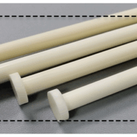


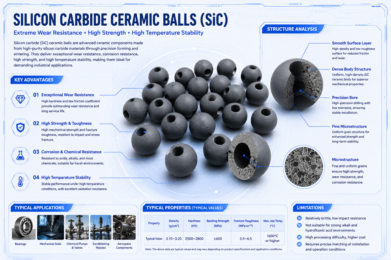


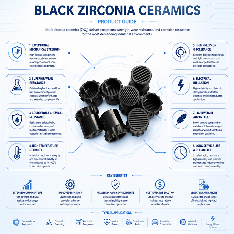
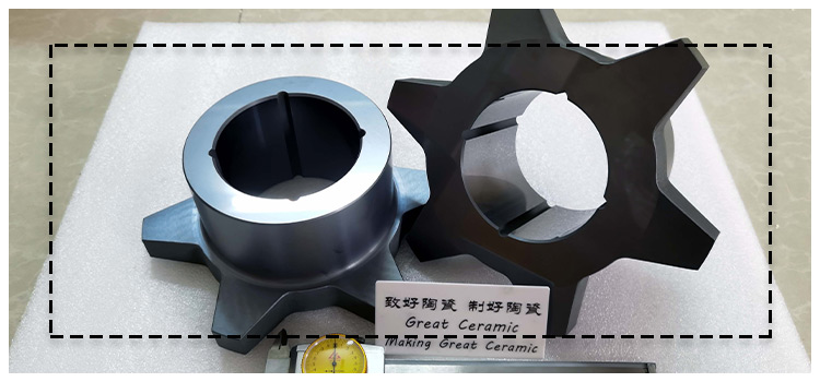


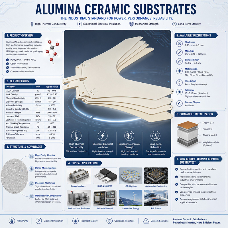


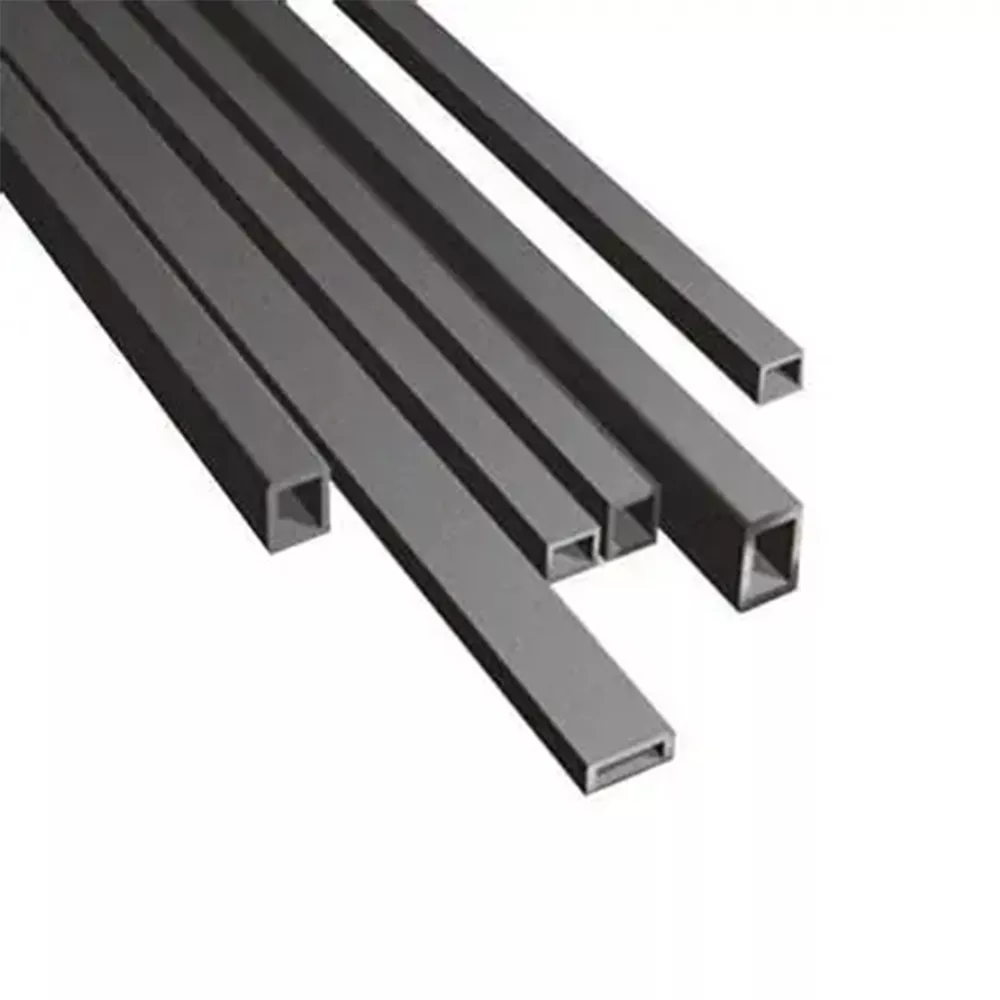
Related Ceramic Products and Quote Requests


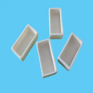


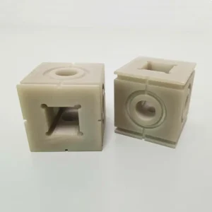


Why Semiconductor Ceramic Components Need Drawing-Led Sourcing
Align material, geometry, functional requirements, and project-specific acceptance details before a quotation discussion begins.
Current Drawing Revision
Share the current drawing revision so dimensions, features, notes, and open questions are discussed against the same controlled part definition.
Material Grade Context
Identify the material designation when known, then relate grade selection to electrical, thermal, chemical, and mechanical conditions for the intended semiconductor application.
Assembly-Critical Geometry
Call out dimensions that govern fit, alignment, clearance, or sealing, helping keep semiconductor ceramic components connected to their mating parts and assembly function.
Functional Surface Requirements
Specify surfaces exposed to contact, motion, vacuum, process media, or electrical interfaces so finishing expectations can be reviewed in the context of use.
Process Route Discussion
Discuss the part features and intended material early, allowing the production route to be considered alongside geometry, surfaces, and project requirements.
Acceptance Evidence Defined
State the inspection records, documentation, and acceptance criteria needed for approval, distinguishing required evidence from general material information before project commitment.
Semiconductor Ceramic Components to Explore
Explore material families, component forms and application paths, then define the drawing, service conditions and acceptance criteria for your project.
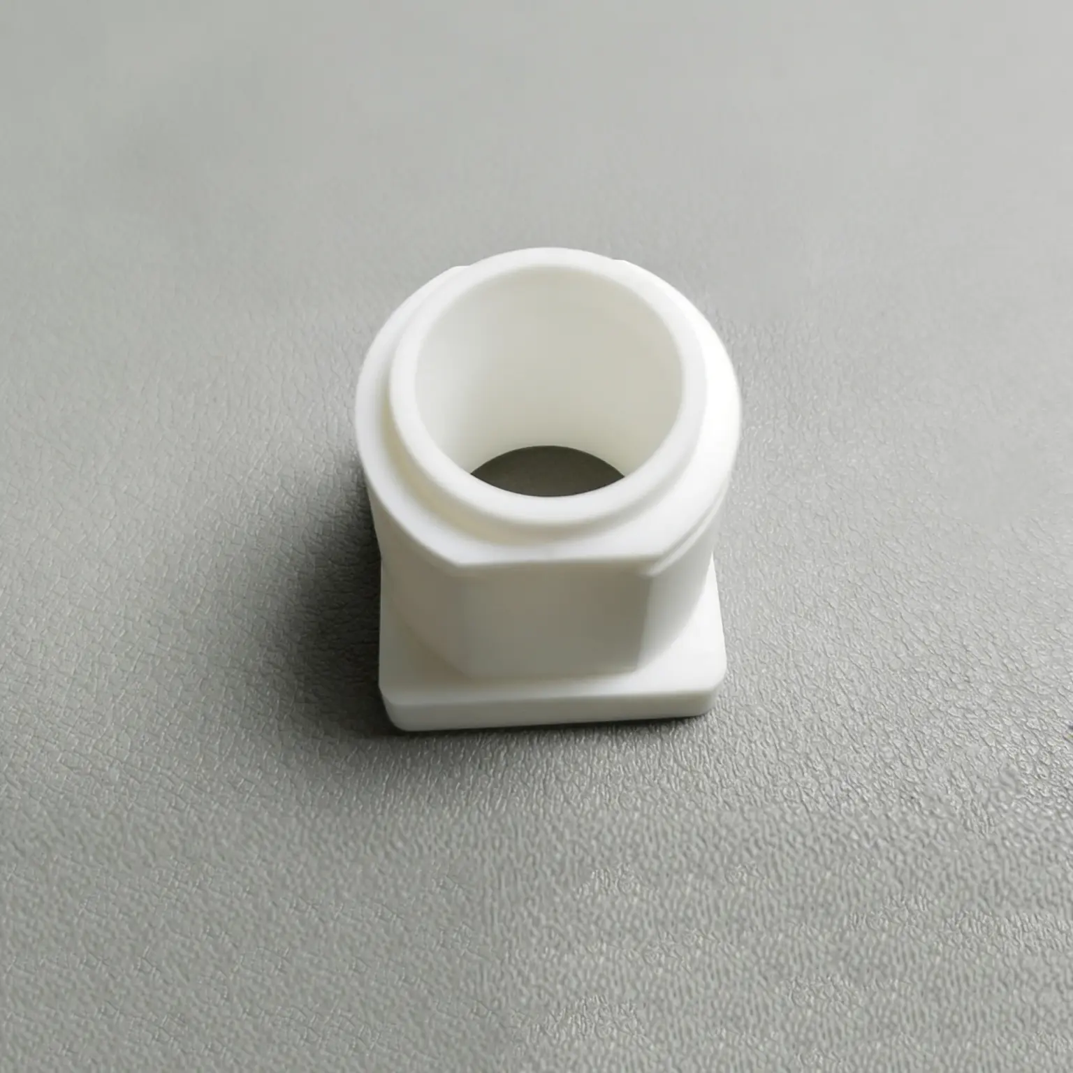
Ceramic Manufacturing Capabilities
Review ceramic manufacturing capabilities against the part requirement: forming route, machining needs, critical dimensions, mating surfaces and inspection expectations. Share the current drawing revision, quantity and acceptance criteria so a quotation discussion is based on the component rather than a material name alone.
Discuss Your Ceramic Part
Ceramic Solutions by Industry
Explore advanced ceramics applications by the operating challenge, including electrical insulation, wear, heat, chemical exposure and semiconductor process environments. Industry context helps identify relevant component geometry, material family and documentation needs, but final suitability depends on the specific assembly and service conditions.
Discuss Your Ceramic Part
Advanced Ceramic Materials
Compare advanced ceramic materials including alumina, zirconia, silicon carbide, silicon nitride, aluminum nitride and boron nitride. General material data is a starting point; confirm the grade, dimensions, processing route and project-specific acceptance requirements before selecting a part specification.
Discuss Your Ceramic Part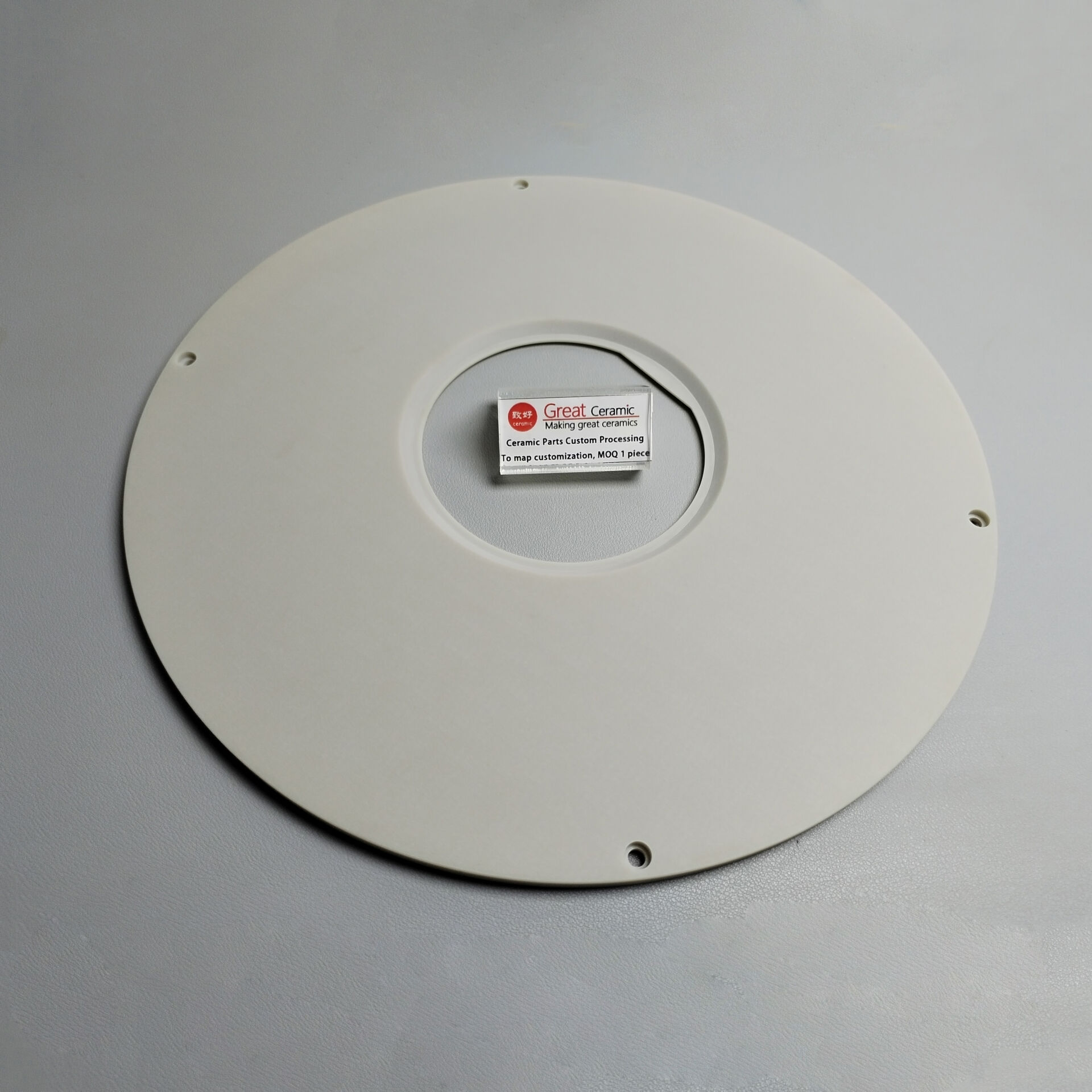
Technical Ceramic Products
Browse technical ceramic products and industrial ceramic parts by familiar forms such as tubes, rods, rings, plates, substrates, and custom machined components. For replacements or new assemblies, identify fit surfaces, assembly-critical dimensions, operating environment, and drawing details needed to evaluate the requirement.
Discuss Your Ceramic Part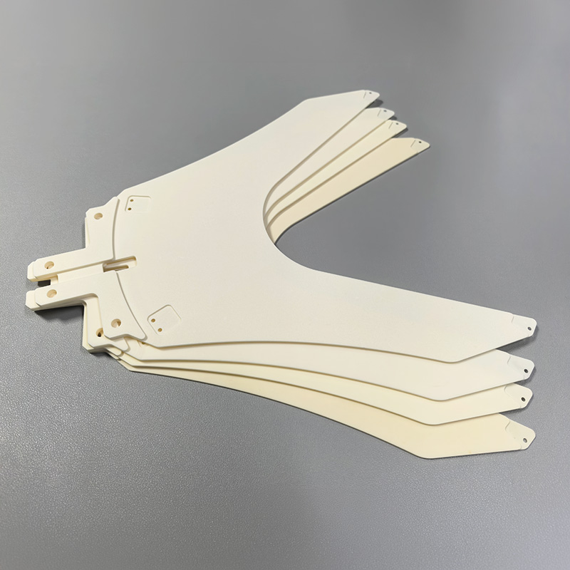
Technical Ceramic Resources
Use this technical ceramics guide to structure a clearer inquiry: material designation if known, drawing revision, quantity, service conditions, critical tolerances and required documentation. Email a drawing to info@zlrsmaterials.com or contact Porcecore on WhatsApp at +86 130 6482 5920 to discuss open requirements.
Discuss Your Ceramic PartSemiconductor Ceramic Components: Materials to Discuss
Alumina Ceramics
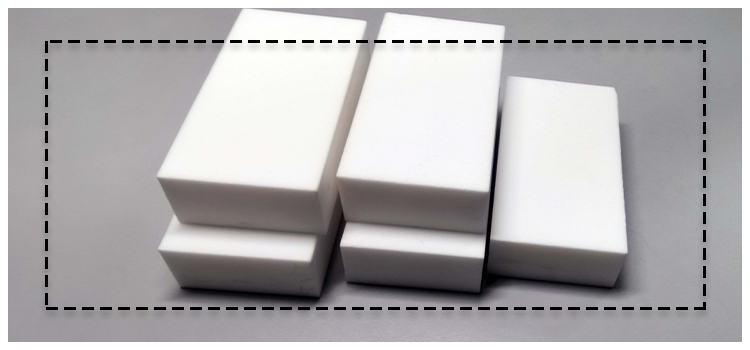
A widely considered option for insulating tubes, rings, substrates, and handling parts. Electrical insulation and dimensional stability can support many equipment requirements, subject to grade, geometry, finish, and project-specific confirmation.
Zirconia Ceramics
Often discussed for guides, seals, and wear-facing mechanical parts where toughness is an important consideration. Review the stabilized grade, contact surfaces, operating environment, and inspection expectations against the current drawing.
Silicon Carbide Ceramics
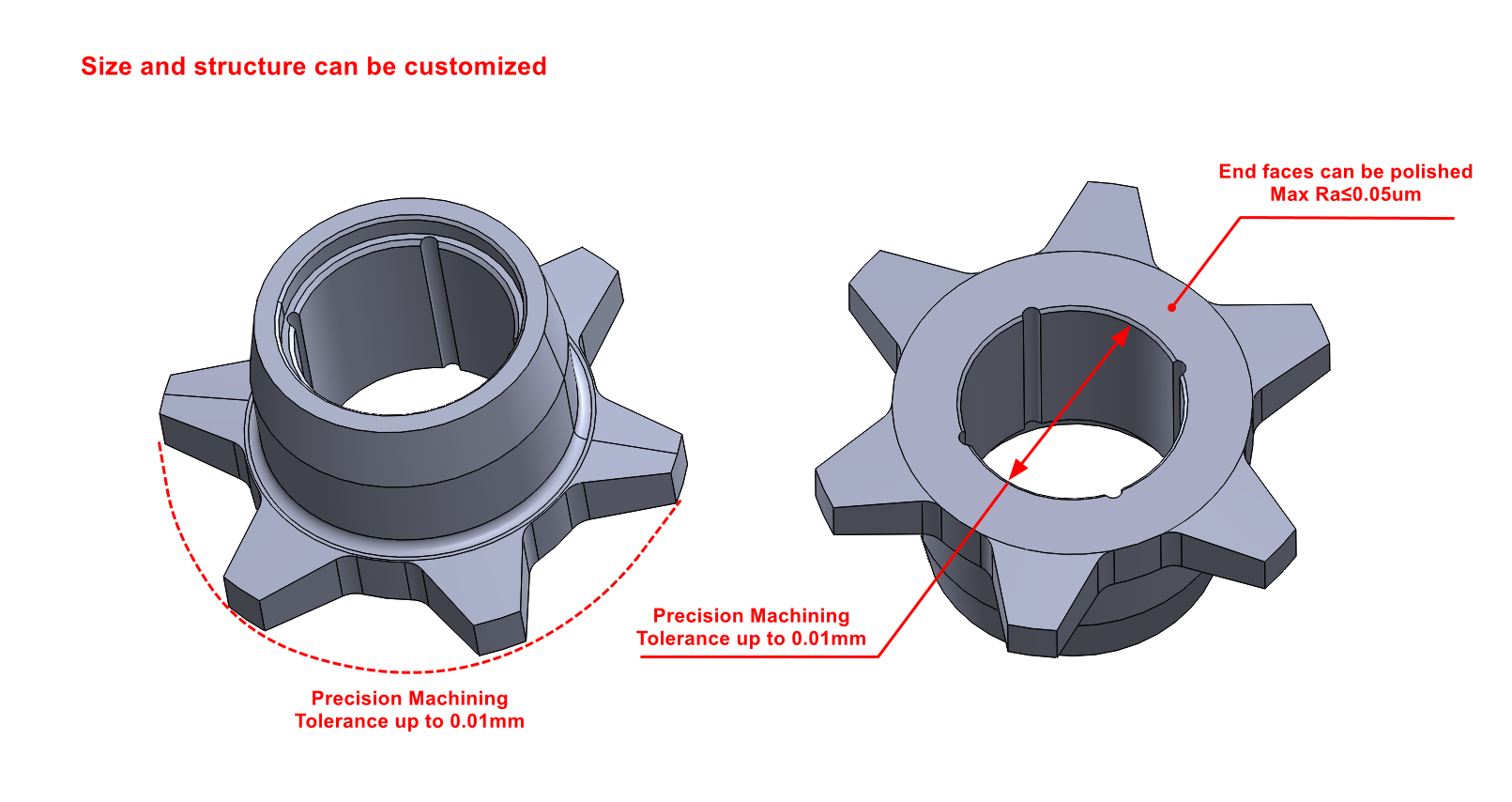
A material family to evaluate for chamber-facing, thermal, or structurally demanding components. Its selection should be tied to the process environment, required geometry, surface condition, contamination considerations, and acceptance criteria.
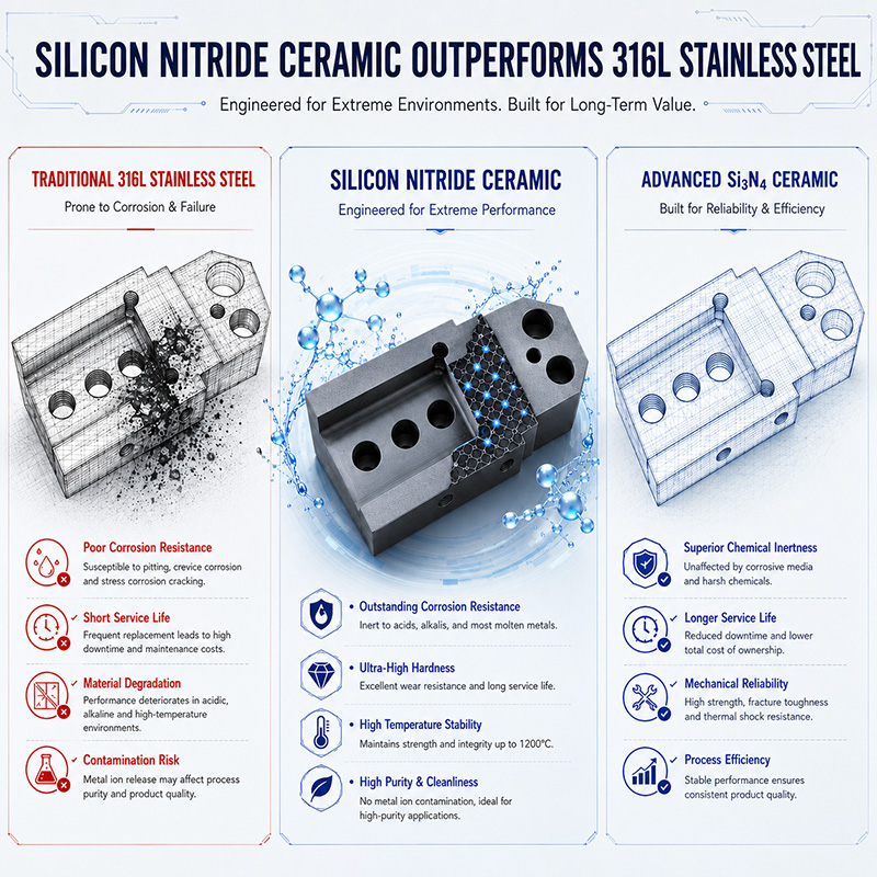
Silicon Nitride
Consider for structural components, guides, and insulating parts exposed to mechanical loading or temperature changes. Define the material designation, critical dimensions, assembly interfaces, service conditions, and documentation needed before quotation.
Aluminum Nitride
Commonly explored for heat-management substrates, insulating parts, and electronic equipment components. Thermal requirements, electrical needs, thickness, mounting interfaces, and handling conditions should guide the material and part discussion.
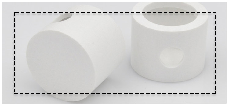
Boron Nitride
A specialty ceramic family to discuss for selected thermal, electrical, or high-temperature component requirements. Clarify the application, material form, atmosphere, geometry, and any fit-critical surfaces before defining a sourcing path.
Semiconductor Ceramic Components: Processes to Discuss
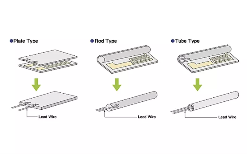
Ceramic Forming
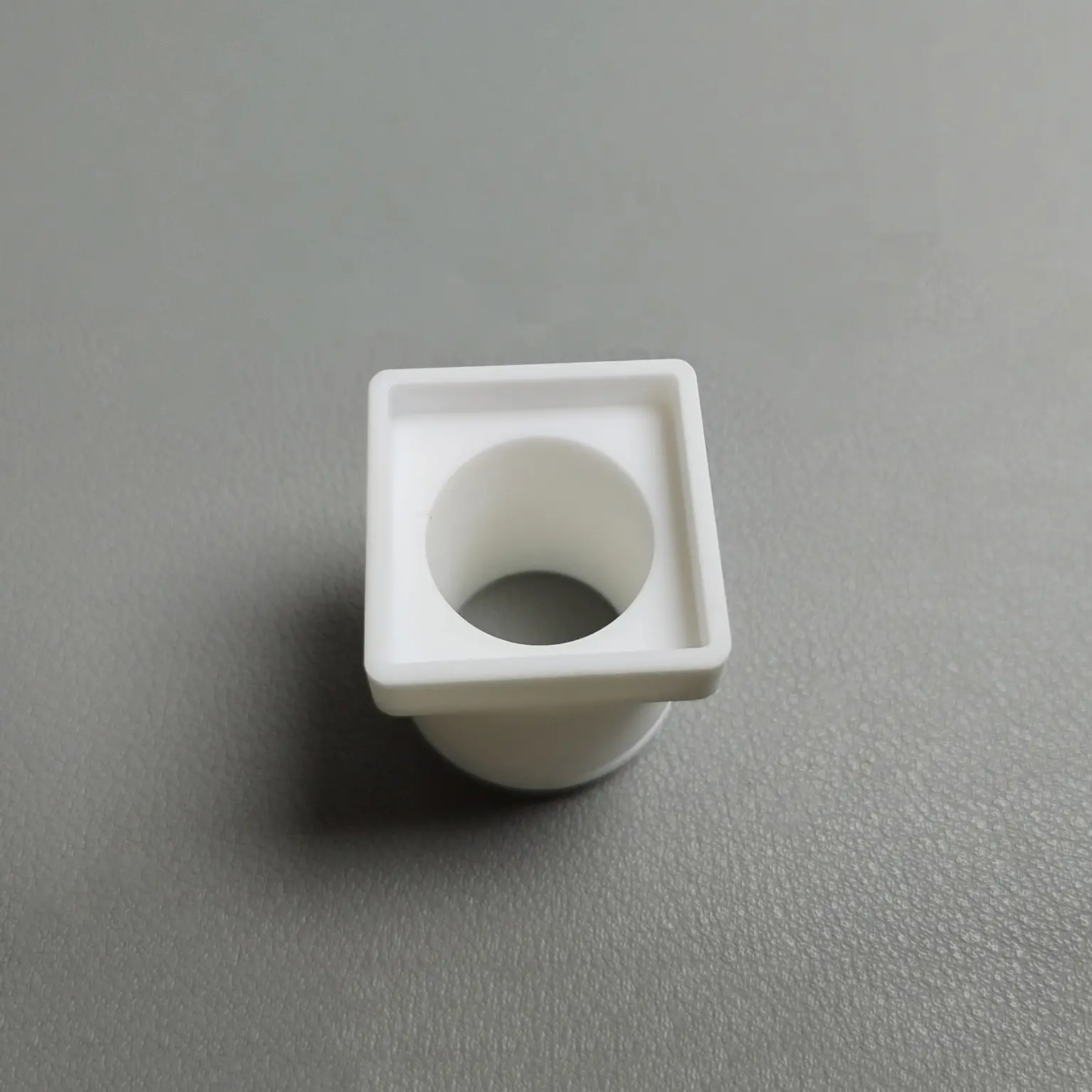
Discuss a forming approach in relation to part geometry, wall sections, volume expectations, and material family. Early review can help identify which features should be considered before sintering and subsequent finishing.
Green Machining
For selected geometries, features may be reviewed before final densification. Share holes, slots, contours, and critical dimensions on the current drawing so the sequence can be evaluated alongside tolerance and surface requirements.

Precision Machining
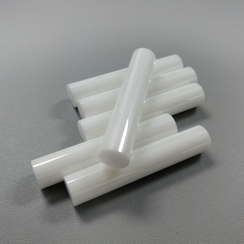
Post-sintering machining discussions focus on the surfaces, profiles, openings, and interfaces that determine assembly. Identify mating features and dimensional priorities so a quotation conversation addresses the part rather than material alone.
Grinding Finishing
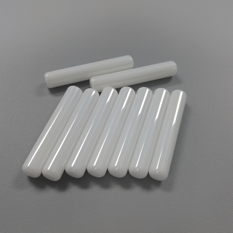
Grinding, lapping, polishing, or other finishing requirements should be tied to specified surfaces and functional needs. Note flatness, parallelism, roughness, edge condition, and any areas where finish affects fit or process performance.
Inspection Planning
Inspection expectations belong with the drawing and acceptance criteria. Clarify critical dimensions, measurement references, documentation needs, and sampling expectations so project-specific requirements can be reviewed before commercial terms are confirmed.
Semiconductor Ceramic Components: Interface Features
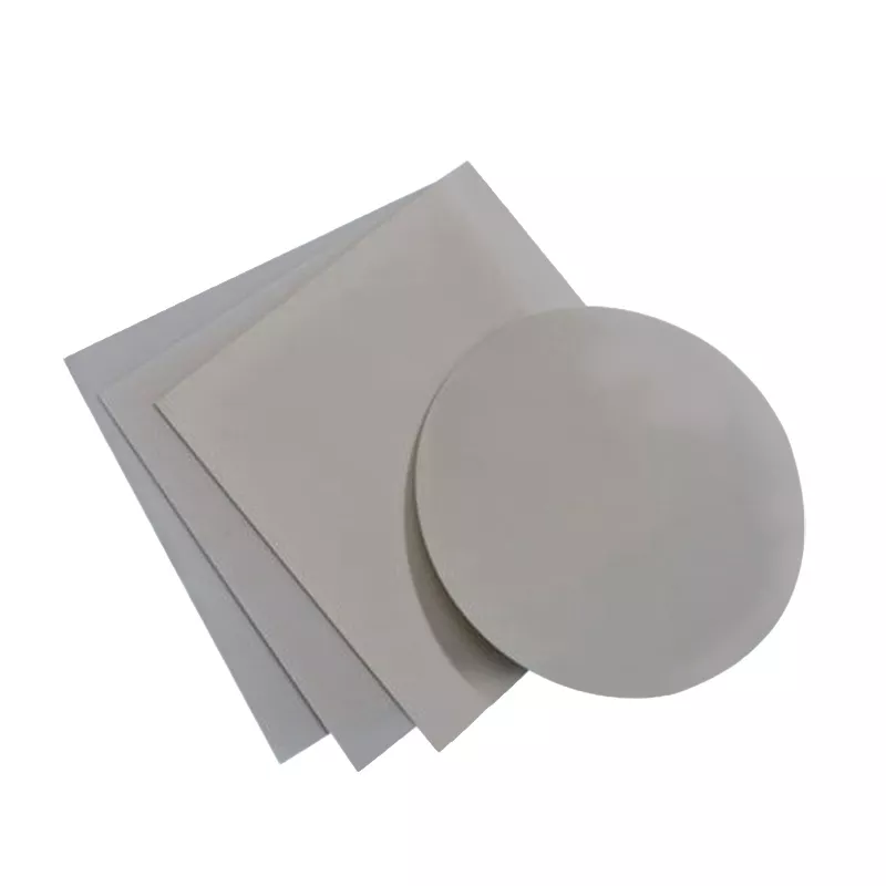
Precision Holes
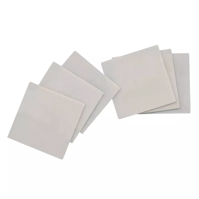
Through-holes, blind holes, and locating features can support mounting, alignment, or fluid and electrical routing. Share diameter, position, depth, mating hardware, and tolerance requirements so compatibility can be reviewed against the drawing.
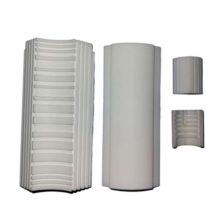
Functional Grooves
Grooves may be considered for sealing, clearance, retention, or routing functions in semiconductor ceramic components. Provide cross-section details, surface requirements, adjacent features, and the operating environment to define the feature appropriately.
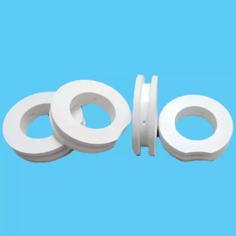
Threaded Interfaces
Threaded or threaded-interface requirements need review with the ceramic geometry, assembly load, mating material, and service conditions. Identify the thread standard, engagement expectations, and whether an insert or alternative fastening approach is required.
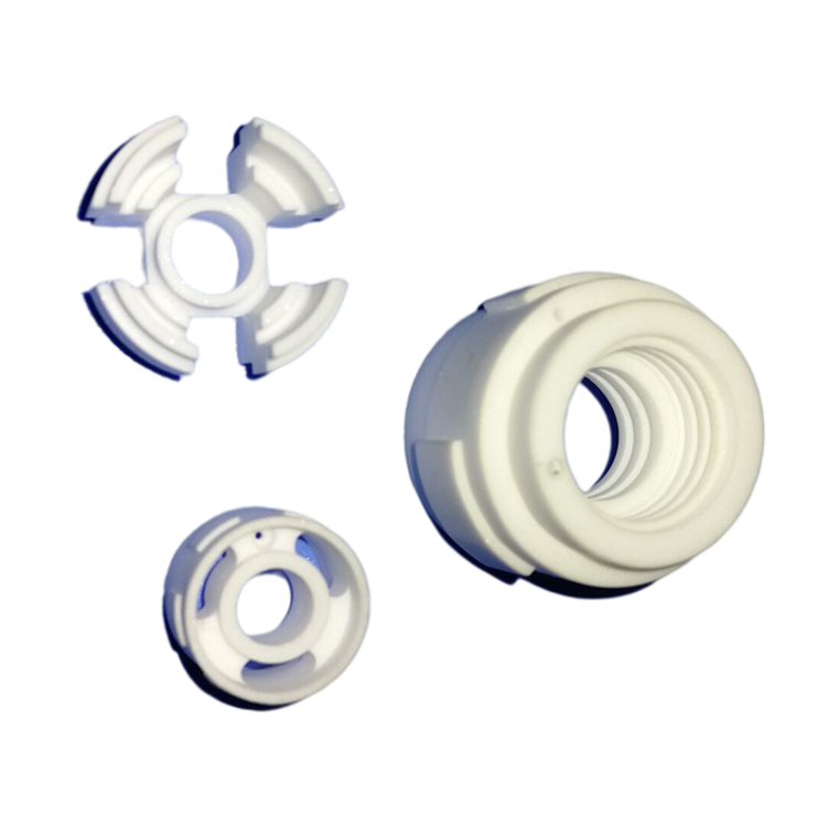
Metallized Surfaces
Metallized interfaces may be relevant where a ceramic part connects with conductive, brazed, or mounted assemblies. Specify the interface area, joining method, electrical role, environmental conditions, and any inspection or documentation expectations.
Part Identification
Identification requirements can include marking locations, traceability references, revision control, or packaging labels. Indicate the required content, placement restrictions, permanence expectations, and whether identification must remain readable after processing or assembly.
Porcecore Semiconductor Ceramic Components
Porcecore was founded by Andy Yuan to make technical ceramic procurement easier to begin and more useful for industrial buyers. We focus on semiconductor ceramic components, industrial ceramic parts, and custom ceramic components, connecting material choices with the specific job a component must perform.
Our scope includes oxide, nitride, carbide, and specialty ceramic families in forms such as tubes, rods, rings, and substrates. Rather than treating a material name as a complete specification, we help project teams frame geometry, mating surfaces, operating conditions, and inspection expectations together.
What distinguishes Porcecore is an application-first, drawing-led approach built on clarity before commitment. Send a current drawing revision, known material designation, quantity, service conditions, and acceptance criteria to give a quotation discussion a practical starting point.

Define Semiconductor Ceramic Components Beyond Material Choice
Start With the Part Job
A material name is only one input. For semiconductor ceramic components, begin with the function, component form, drawing revision, quantity, and service environment so the quotation discussion reflects the part you actually need.
- Identify the component’s intended function
- Share the current drawing revision
- State required quantity and project stage
- Describe the assembly or process context

Map Geometry and Interfaces
Dimensions that govern assembly deserve focused review. Identify bores, threads, grooves, sealing areas, contact faces, and other mating surfaces, then distinguish critical tolerances from preferred dimensions before material and manufacturing details are discussed.
- Mark assembly-critical dimensions
- Identify mating and sealing surfaces
- Call out surface-finish expectations
- Separate essential tolerances from preferences

Describe Operating Conditions
Operating conditions help frame an appropriate project conversation for semiconductor ceramic components. Share temperature exposure, chemical or plasma contact, electrical role, mechanical loads, vacuum conditions, and thermal cycling where known; grade suitability remains subject to project-specific review.
- Note temperature range and cycling
- Describe chemical or plasma exposure
- Clarify insulation or conductivity needs
- Identify loads, vacuum, and wear conditions

Set Acceptance Expectations
Clear acceptance requirements reduce uncertainty before commitment. Include inspection points, material designation if known, documentation needs, packaging expectations, delivery timing, and commercial requirements so open questions can be identified before a project-specific quotation is discussed.
- Define inspection and acceptance criteria
- Specify documentation requirements
- Confirm packaging and delivery needs
- Flag approval and commercial conditions

Why Discuss Semiconductor Ceramic Components from the Drawing Forward
Porcecore helps structure the project conversation around the part, its interfaces, service conditions, and acceptance needs before commitment.
← Swipe left or right to view →
A Clear Path for Semiconductor Ceramic Components
Move from an initial drawing to a defined quotation discussion with the requirements that matter to your project.
Share Part Information
Send the current drawing revision, material designation if known, quantity, application, and service conditions for the semiconductor ceramic component under review.
Define Critical Requirements
Identify assembly dimensions, mating surfaces, tolerances, operating environment, inspection expectations, and any documentation needed for internal approval or incoming acceptance.
Review Material Options
Discuss suitable ceramic families in relation to the part function, geometry, thermal, electrical, mechanical, and chemical exposure requirements described.
Clarify Quotation Basis
Align on the proposed requirement scope before pricing discussion, including grade, dimensions, acceptance criteria, quantity assumptions, and open technical questions.
Confirm Project Terms
Confirm project-specific specifications, documentation, delivery expectations, and commercial terms before any production order is considered agreed for semiconductor ceramic components.
How to Source Semiconductor Ceramic Components with Porcecore
Move from a defined part requirement to a project-specific quotation conversation with the details that matter for fit, function, and acceptance.
Send Your Current Drawing
Share the latest drawing revision or a clear part sketch, identifying critical dimensions, mating surfaces, and any features that determine assembly or function.
Define Material and Service
Describe the known material designation, operating environment, temperatures, electrical needs, chemical exposure, and mechanical demands so the application context is clear.
Clarify Quantity and Acceptance
State prototype or production quantity, inspection expectations, required documentation, and the dimensions or surface conditions that will be used for approval.
Confirm Project Terms
Review the project-specific discussion covering grade, geometry, tolerances, documentation, delivery expectations, and commercial terms before treating any proposal as an agreed order.
Documentation Requirements for Semiconductor Ceramic Components
Semiconductor Ceramic Components: Project Discussion Scenarios
An equipment builder submits a revised chamber-insulator drawing for 24 pieces, identifies two mating surfaces, and asks to review material options, dimensional tolerances, and inspection documentation before requesting a quotation.
A procurement team requests a replacement ceramic ring for an installed assembly, providing the current drawing, annual quantity estimate, service environment, and acceptance criteria so open technical and commercial questions can be identified early.
A distributor brings a substrate requirement for 50 units and asks Porcecore to clarify the material designation, critical assembly dimensions, required records, and whether the proposed geometry needs further definition before quotation review.
Semiconductor Ceramic Components FAQ
Practical guidance for preparing a drawing-led quotation discussion with Porcecore.
What should I include when requesting a quote for semiconductor ceramic components?
Can Porcecore help select a material for semiconductor ceramic components?
Which drawing details matter most for a ceramic component?
How are tolerances and functional surfaces reviewed?
Can I request prototype, sample, or production quantities?
What inspection evidence can be discussed for semiconductor ceramic components?
How should semiconductor ceramic components be packaged and shipped?
How can I share an IP-sensitive drawing or replacement-part inquiry?
Complete Buyer’s Guide to Semiconductor Ceramic Components
Use this practical framework to match ceramic performance to semiconductor operating conditions, evaluate drawing-based suppliers, compare cost drivers, and avoid specification, quality, and sourcing mistakes that can disrupt equipment reliability.
1. What Are Semiconductor Ceramic Components?
Three functional categories define semiconductor ceramic components: structural parts, electrical insulators, and functional electronic ceramics. They serve wafer processing, chamber assemblies, thermal-management paths, wafer handling, and device packaging.
Structural components include rings, nozzles, arms, fixtures, and chamber-facing parts that must retain geometry under load, heat, vacuum, or reactive process exposure. Insulating components such as feedthroughs, substrates, and spacers separate electrical paths while managing heat; functional ceramics may provide dielectric, sensing, piezoelectric, or conductive behavior.
Five procurement variables deserve early review: material purity, thermal expansion and conductivity, chemical resistance, dimensional stability, and particle-control expectations. A drawing should identify critical mating surfaces, service environment, cleaning requirements, tolerances, and acceptance criteria, because a general material family does not define a qualified part.
2. Evolution of Semiconductor Ceramic Components
1990s-era semiconductor tools already relied on technical ceramics where metals or polymers could not reliably tolerate heat, chemicals, or electrical isolation requirements. As vacuum processing and plasma etch became more demanding, components increasingly required controlled purity, surface finish, and geometry rather than a general industrial material designation.
1 micrometer-scale flatness is an example of the precision now associated with selected semiconductor ceramic parts, while chamber-facing surfaces must also limit particle generation and withstand process exposure. https://www.ceramtec-industrial.com/en/products-applications/semiconductor-industry
2 nm-class process development and tighter process windows increase the importance of fit-critical dimensions, traceable inspection criteria, and repeatable material-grade selection. Current sourcing therefore prioritizes the drawing revision, mating surfaces, vacuum or plasma conditions, thermal cycle, cleanliness expectations, and documentation needed to support equipment uptime.
3. Types of Semiconductor Ceramic Components
Six common families of semiconductor ceramic components serve distinct process, thermal, electrical, and handling functions. Classifying the part first helps purchasers request the interfaces and inspection features that matter.
Wafer Support And Chamber Parts
Wafer chucks and carriers position wafers during processing; flatness, vacuum features, contact lands, and datum scheme drive manufacture and inspection.
Focus rings and chamber liners face plasma, chemical exposure, and thermal cycling. Specify wall thickness, erosion-critical surfaces, joint geometry, and allowable edge break.
Electrical And Gas Components
Insulators and feedthroughs isolate electrical paths across chamber boundaries; sealing diameters, metallized areas, concentricity, and leak-test criteria require drawing definition.
Nozzles and gas-distribution parts control gas delivery under chemical exposure. Define hole quantity, diameter, pattern datum, internal passages, surface finish, and cleaning expectations.
Thermal And Handling Parts
Substrates and heat-management parts transfer or isolate heat while supporting electrical assemblies. Identify mounting faces, thickness, flatness, thermal interfaces, and any plated or patterned regions.
Handling end effectors carry wafers through repeated motion and contact. Specify pickup locations, clearances, stiffness-critical sections, contact finish, and particle-control acceptance criteria.
4. Materials for Semiconductor Ceramic Components
Material selection starts with the process window: voltage, heat flux, plasma chemistry, thermal cycling, load, and particle-risk limits. No single semiconductor ceramic components material is best across every chamber or assembly.
| Material | Primary Advantage | Key Watchpoint | Relative Cost |
|---|---|---|---|
| Alumina | Insulation; machinable | Lower heat transfer | Low |
| Aluminum nitride | Thermal conductivity; insulation | Higher cost; handling | High |
| Silicon carbide | Plasma, chemical resistance | Difficult machining | High |
| Silicon nitride | Strength; toughness | Grade-dependent purity | High |
| Zirconia | Toughness; wear resistance | Higher expansion | Medium-high |
| Quartz | Purity; chemical resistance | Lower toughness | Medium |
Selection By Service Conditions
AlN combines electrical insulation with high heat transfer for thermal-management interfaces; alumina suits many insulating, cost-sensitive parts. Source: https://www.ceramtec-industrial.com/en/products-applications/semiconductor-industry
Plasma And Mechanical Tradeoffs
SiC favors rigid, low-expansion plasma-exposed hardware; silicon nitride adds fracture toughness for loaded, thermally cycled parts. Zirconia favors toughness and wear, while quartz is relevant where purity and thermal-processing compatibility govern.
Specification Before Grade
Purity, porosity, grain structure, finish, and machining route can change performance within one material family. Specify mating surfaces, chemical exposure, electrical duty, and acceptance criteria before comparing relative cost.
5. Custom Semiconductor Ceramic Components
One current drawing revision turns a custom ceramic request into an engineering review. Semiconductor ceramic components should be defined by interface surfaces, process environment, and acceptance criteria rather than a catalog material name.
Geometry And Internal Features
Every hole, channel, radius, and thin wall should carry a functional dimension and datum. Deep internal features or sharp transitions can increase machining difficulty, breakage risk, inspection time, and lead time.
Interfaces And Surface Requirements
Each mating face needs its required finish, flatness, parallelism, and allowable tolerance stated on the drawing. Threads, metallized areas, and bonded assemblies require compatible geometry plus defined inspection and handling expectations.
Documentation And Packaging
A complete package identifies material designation, quantity, revision control, inspection records, and clean packaging needs. Early agreement on critical dimensions and packaging reduces quotation ambiguity, protects yield planning, and avoids preventable rework.
6. Quality Requirements That Protect Process Stability
100% of release requirements should be tied to function: assembly fit, contamination risk, vacuum exposure, or electrical behavior. Put measurable limits on the drawing or purchase order, then confirm the inspection method and sampling basis.
Traceability And Material State
Each lot should link the part number, drawing revision, material designation, and inspection record.
Density, open porosity, and purity need stated limits only when the service environment makes them critical; a generic material-family label is not enough.
Surfaces, Edges, And Dimensions
Ra, flatness, parallelism, bore size, and datum-based dimensions should be specified for mating or process-facing surfaces.
Edge-break size and permitted chips should be defined where handling, sealing, or particle release depends on them; cosmetic limits elsewhere can add cost without improving function.
Clean Release Packaging
Final cleanliness should identify residue, particle, and handling expectations appropriate to the installation environment.
Packaging should protect critical faces, prevent part-to-part contact, and preserve lot identification through receipt; require a documented inspection report when qualification needs objective evidence.
7. Choosing a Semiconductor Ceramic Components Supplier
Two supplier reviews should occur before award: one for application fit and one for production control. Compare semiconductor ceramic components against the actual drawing, service environment, and acceptance plan—not a catalog claim.
Assess Technical Fit
First, ask how the supplier reviews material grade, geometry, mating surfaces, thermal load, vacuum or chemical exposure, and particle-risk assumptions. Confirm machining routes for holes, threads, grinding, lapping, and fragile features, plus metrology methods for critical dimensions.
Request Evidence And Control
Second, define required inspection records, material traceability, certificates, first-article expectations, and nonconformance handling. Ask how drawing revisions, approved deviations, process changes, and subcontracted operations are communicated and controlled.
Build A Complete RFQ
Third, provide the current drawing revision, known material grade, tolerances, surface requirements, operating environment, annual and release quantities, inspection requirements, documentation, delivery dates, and packaging needs. Request a prototype-to-production plan, realistic capacity discussion, and named technical contact before committing.
8. Common Semiconductor Ceramic Components Sourcing Mistakes
A material name, a drawing, and a unit price do not define a usable ceramic part. Before release, convert each assumption into a measurable requirement for the actual service environment.
Material Without Service Conditions
Alumina, silicon carbide, or aluminum nitride alone leaves critical selection questions open. The consequence can be cracking, corrosion, heat-transfer failure, or particle generation.
Ask: What temperatures, thermal cycles, gases, chemicals, vacuum level, electrical duty, and mechanical loads will this part see?
Unclear Drawing And Surface Requirements
A tolerance without datums, mating surfaces, roughness, edge condition, or cleanliness definition is ambiguous. The consequence is an assembly mismatch or a part that passes dimensional checks but disrupts the process.
Ask: Which dimensions control assembly, what datum scheme applies, and what surface, cleaning, packaging, and particle criteria are required?
Price-Only Sample Approval
A low unit price can conceal impractical geometry, yield risk, inspection gaps, or inadequate documentation. An unqualified sample may not represent repeat production.
Ask: Is the geometry manufacturable, and which material, dimensions, inspection methods, records, and acceptance limits must production meet?
9. From Drawing to Qualified Production
A qualified program moves through defined decisions, not a single purchase order. Engineers, procurement, equipment builders, and distributors should assign ownership before samples or production commitments begin.
Define The Operating Envelope
First, record temperature, vacuum or atmosphere, chemicals, electrical duty, loads, and allowable contamination risk.
Next, identify mating parts, installation constraints, expected life, and the failure modes the component must avoid.
Freeze Requirements Before Sampling
Second, issue the current drawing revision with critical dimensions, datum scheme, surface requirements, quantity, and acceptance criteria.
Then request a manufacturability review covering geometry, material designation, tolerances, machining access, and inspection method. Resolve open items in writing before prototype release.
Qualify And Control Production
Third, approve prototype samples against agreed dimensional and material-related evidence, then validate function in the intended equipment.
Finally, define production controls, change notification, lot documentation, packaging, reorder point, and replenishment forecast. Procurement should preserve the approved revision and acceptance record.
10. Semiconductor Ceramic Components Pricing and Cost Drivers
3 cost layers shape a quote: material grade and blank size establish the starting point, while complex geometry and thin sections increase machining time.
2 finishing decisions—surface finishing and tighter tolerances—can add grinding, lapping, polishing, or more inspection steps. An accurate quote needs the current drawing, operating requirements, acceptance criteria, and packaging needs.
| Quantity tier | Primary cost drivers | Typical lead-time influence |
|---|---|---|
| 1–5 pieces | Tooling, setup, material yield, first-article inspection | Drawing clarification and process planning can dominate |
| 6–50 pieces | Geometry, tolerance stack, surface finish, inspection level | Repeatable machining and inspection reduce scheduling friction |
| 51–250 pieces | Quantity, fixture amortization, packaging, lot documentation | Dedicated fixtures and packaging planning may be justified |
| 250+ pieces | Material purchasing, process capability, packaging format | Forecast stability and approved samples support production planning |
Discuss Your Semiconductor Ceramic Components Requirement Today
Email your drawing, operating environment, material preferences, quantity, and acceptance criteria to begin a clear project discussion.